
On May 21, 2026, AMD paired two related announcements: it said its 6th Gen EPYC server CPU, codenamed Venice, has entered production ramp on TSMC’s 2nm process, and it said it will invest more than $10 billion across Taiwan’s ecosystem to expand packaging, manufacturing and partner capacity for next-generation AI infrastructure. Together, the updates turn AMD’s AI push into more than a roadmap story. The company is trying to lock in the silicon, packaging and rack-scale supply chain needed to ship larger agentic AI systems at volume.
The immediate headline is the Venice ramp. AMD said the chip is the first high-performance computing product in the industry to enter production on TSMC’s advanced 2nm technology. But the more important business signal may be everything around it: advanced packaging, interconnect bandwidth, ODM relationships and a broader manufacturing footprint that includes future ramp plans at TSMC Arizona.
What AMD announced on May 21
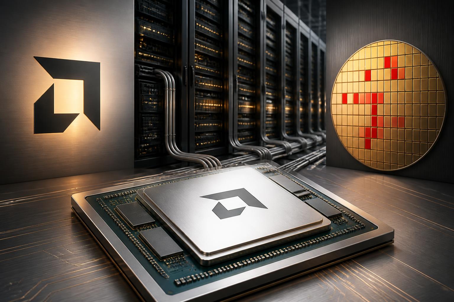
AMD’s first announcement focused on Venice, the next-generation EPYC data center CPU in its 6th Gen lineup. The company said production is ramping in Taiwan on TSMC 2nm and that the processor is aimed at the cloud, enterprise, HPC and AI infrastructure workloads that increasingly depend on higher efficiency and tighter system-level integration.
In the same day’s broader infrastructure announcement, AMD said it will invest more than $10 billion across the Taiwan ecosystem to deepen strategic partnerships and scale advanced packaging capabilities for AI systems. AMD tied that spending to several concrete pieces of infrastructure: EFB-based 2.5D packaging, panel-based interconnect work with PTI, collaboration with ASE and SPIL, and manufacturing support from server and system partners including Sanmina, Wiwynn, Wistron and Inventec.
AMD also linked these efforts directly to its upcoming Helios rack-scale platform, which it said is on track for multi-gigawatt deployments beginning in the second half of 2026. That platform is expected to combine Venice CPUs with AMD Instinct MI450X GPUs, networking and the ROCm software stack.
Why the packaging and manufacturing angle matters more than another chip milestone
It is easy to read this as a simple CPU manufacturing update, but AMD is framing it as a response to a different bottleneck. As model training, inference and long-running agent workflows scale, the challenge is no longer only raw compute. It is whether vendors can deliver integrated systems with enough memory bandwidth, interconnect efficiency, power discipline and assembly capacity to move from announcements to real deployments.
That is why AMD spent so much of the day talking about advanced packaging. The company highlighted EFB-based 2.5D bridge technology as a way to increase interconnect bandwidth and improve power efficiency, and said its work with PTI qualified what it called the industry’s first 2.5D panel-based EFB interconnect. In practice, AMD is signaling that packaging economics and manufacturability are becoming central to AI infrastructure competition.
AMD also used the Venice release to push its next step. It said a follow-on EPYC processor, Verano, will extend TSMC 2nm further across the roadmap and add LPDDR-based memory innovations designed for increasingly power-constrained cloud and AI environments. That matters because AI infrastructure buyers are starting to judge platforms less on isolated chip specs and more on how well whole racks balance compute, memory, networking and operating cost.
Business impact for enterprise AI and agent deployments
For enterprises, the biggest takeaway is not that a new EPYC chip is coming. It is that AI infrastructure is becoming a supply-chain and systems-integration problem again. If AMD can execute on Venice, Helios and its Taiwan packaging strategy, it strengthens its case that customers should evaluate rack-scale alternatives rather than defaulting to a single-vendor AI stack.
That matters most for buyers planning large inference fleets, internal agent platforms and hybrid enterprise deployments. Agentic workloads put unusual pressure on data movement, orchestration, memory access and cost per useful action. CPUs remain critical in that stack because they coordinate storage, networking, scheduling, security and system control around the accelerators doing model execution.
AMD’s mention of future production at TSMC Arizona also broadens the story beyond Taiwan. It suggests the company wants a more geographically diversified manufacturing base as AI infrastructure buyers care more about resilience, procurement flexibility and domestic supply options alongside performance.
The Reuters summary of the investment announcement captured the market context well: AMD is widely viewed as one of the leading challengers to Nvidia in AI chips, and Taiwan remains one of the most important centers in the global AI supply chain. May 21’s announcements do not change the leaderboard by themselves, but they do show AMD trying to compete with a fuller infrastructure play instead of a narrower chip-only argument.
What to watch next
The next proof points are operational, not rhetorical. First, watch whether Helios deployments in the second half of 2026 materialize at the scale AMD is describing. Second, watch whether AMD can turn its packaging partnerships into visible delivery advantages rather than engineering talking points. Third, watch whether Arizona ramp plans become meaningful enough to change how U.S. enterprise buyers think about sourcing advanced AI infrastructure.
For AI agents and enterprise automation teams, the practical implication is straightforward: the infrastructure race is moving below the model layer. The winners will not be decided only by benchmark scores or chatbot mindshare. They will also be decided by who can ship the racks, package the silicon, move the data fast enough and keep power and deployment economics under control when agent workloads become real production traffic.